Email: info@yycheme.com Tel: +86-19304758719


Email: info@yycheme.com Tel: +86-19304758719
As a leading supplier of high-purity specialty industrial gases and advanced electronic chemicals, we understand that staying informed on critical supply chain materials is essential for our global semiconductor partners. Today, we’re breaking down one of the most strategically important specialty gases in the AI era: Tungsten Hexafluoride (WF₆).
What Is Tungsten Hexafluoride?
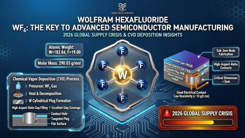
Tungsten Hexafluoride (WF₆, CAS 7783-82-6) is an inorganic specialty gas and the only stable, commercially viable tungsten fluoride used in semiconductor manufacturing. At room temperature it is a colorless, pungent toxic gas; in liquid form it appears pale yellow, and as a solid it forms white, hygroscopic crystals. It is one of the heaviest gases in the world, with a gas density of approximately 12.7g/L—about 10 times denser than air.
Chemically, WF₆ is highly reactive: it acts as a strong fluorinating and oxidizing agent, corroding nearly all metals except nickel, Monel alloy, stainless steel, gold and platinum. It hydrolyzes rapidly upon contact with water, producing highly toxic hydrogen fluoride (HF) and tungsten trioxide, and fumes visibly in humid air.
Why Is WF₆ Indispensable?
WF₆ is the only commercially available precursor for depositing tungsten metal films via Chemical Vapor Deposition (CVD) and Atomic Layer Deposition (ALD) processes, accounting for over 90-95% of global demand.
To put it simply: modern chips are like nanoscale 3D cities, with tens of billions of transistors that need to be connected via metal wiring. WF₆ enables the growth of high-purity tungsten films inside nanoscale deep holes, perfectly filling ultra-fine contact holes and vias to build the conductive bridges between transistors and external circuits.
Key application scenarios include:
· Advanced logic chips: Contact hole filling and tungsten plug preparation for 7nm/5nm/3nm processes; single-wafer WF₆ consumption for 3nm chips is 2.5x that of 28nm chips.
· 3D NAND flash memory: Filling vertical vias; consumption scales with layer count—200+ layer stacks require 6N-grade purity, while 500+ layer stacks require 7N-grade purity.
· HBM (High Bandwidth Memory): Multi-layer interconnect structures mean single-chip tungsten consumption is 3x that of standard chips.
· DRAM memory: Used for capacitor structures and bitline conductive layers.
2026 Global Supply Crunch: By the Numbers
As of 2026, the global WF₆ market is in a severe seller’s market, with spot supply extremely scarce.
On the supply side, Japan’s Kanto Denka and Central Glass permanently ceased production on July 1, 2026 due to high-purity tungsten powder feedstock shortages, cutting approximately 25% of global high-end capacity (2000-2200 metric tons/year) from the market. South Korean producers prioritize domestic chipmakers, with export volumes continuously shrinking.
On the demand side, AI computing demand has driven explosive growth in HBM and 3D NAND production. As 3D NAND stacks scale beyond 300 layers, single-wafer WF₆ consumption has jumped from 0.8kg to over 2.5kg; HBM chips consume 3x the tungsten of standard chips.
The global supply-demand gap is stark: 2026 global demand is estimated at 7500-8000 metric tons, while effective global supply is only ~6700 metric tons, creating a rigid annual shortfall of 800-2000 metric tons.
Prices have surged accordingly: 6N-grade WF₆ has jumped from under 500,000 RMB/ton at the start of 2026 to 2.2-3.6 million RMB/ton (a 190%+ increase), while 7N-grade spot prices for urgent orders have exceeded 4.8-5 million RMB/ton—a more than 5x increase year-to-date. New production lines require 18-30 months for construction and wafer fab customer certification, so the supply gap is not expected to ease until late 2027 to 2028. 1, 2, 3
China’s Role in the Global Supply Landscape
China’s share of global WF₆ capacity is projected to rise from 46% in 2025 to 80% by 2027, reshaping the global supply map. CSSC Special Gas currently leads global production with 2000 metric tons/year of capacity, capable of stably producing 7N-grade product for top domestic and overseas wafer fabs. 1, 2
Purity Grades & Application Matching
· 5N grade (99.999%): Mature process chips, general materials R&D.
· 6N grade (99.9999%): 14-7nm processes, standard HBM, 200+ layer 3D NAND.
· 7N grade (99.99999%): 3-2nm advanced processes, high-end HBM, with impurity control down to the parts-per-billion level. 5, 14
In short, while WF₆ accounts for a small fraction of total chip manufacturing costs, it carries extremely high strategic weight: a supply disruption can force multi-billion-dollar advanced wafer fabs to halt production entirely. As the AI computing race continues to accelerate, this "niche specialty gas" has become the choke point for global advanced chip manufacturing.
As a trusted specialty gas supplier, we maintain strict quality control and stable supply of high-purity WF₆ to support our partners’ production needs. For product specifications, certification documentation or export inquiries, please reach out to our team directly.

Contact: Jiang.S
Phone: +86-19304758719
E-mail: info@yycheme.com
Whatsapp:+86-18966258719
Add: Liushi Town, Yueqing City, Wenzhou City, Zhejiang Province, 325604, China