Email: info@yycheme.com Tel: +86-19304758719


Email: info@yycheme.com Tel: +86-19304758719
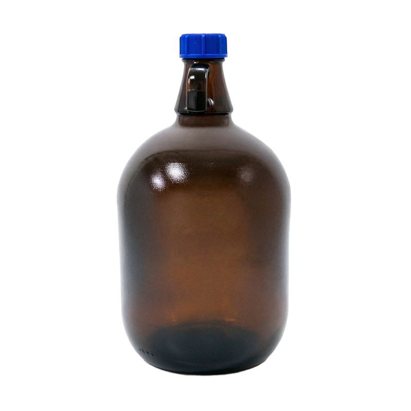
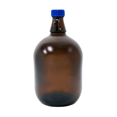
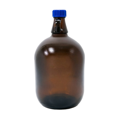
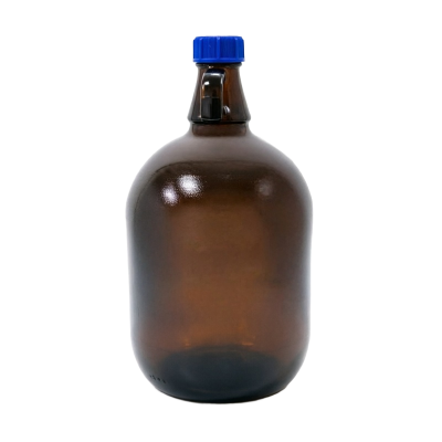
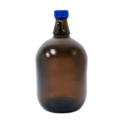
Our G-line positive photoresist series is engineered for 405nm wavelength exposure, based on the mature Novolac resin / DNQ (Diazonaphthoquinone) photosensitive system. Designed for cost-effective lithography at G-line wavelength, this series delivers reliable performance with ultra-low metal ion contamination (≤10ppb), high resolution, and exceptional adhesion to a wide range of substrates. It is the ideal choice for LED manufacturing, power semiconductor devices, MEMS fabrication, and advanced packaging applications where G-line exposure tools are preferred.
· High Resolution: Achieves critical dimensions down to 0.5μm, suitable for fine patterning in LED, power device, and MEMS manufacturing.
· Ultra-High Purity: Metal ion content controlled at ≤10ppb, preventing contamination during wafer fabrication and ensuring high device yield.
· Excellent Adhesion: Strong bonding to silicon, silicon dioxide, metals (Al, Cu, Ag), and dielectric substrates, ensuring reliable pattern transfer during wet and dry etching processes.
· Wide Process Window: Generous depth of focus (DOF) and exposure latitude for high yield and process stability in mass production.
· Cost-Effective: Optimized formulation provides excellent sensitivity at 405nm, reducing exposure time and improving throughput on G-line steppers and aligners.
Parameter | Specification |
Exposure Wavelength | 405nm (G-line) |
Resolution | 0.50 – 1.0 μm |
Film Thickness | 0.5 – 3.0 μm (adjustable by viscosity and spin speed) |
Metal Ion Content | ≤10 ppb |
Developer | 2.38% TMAH (aq.) or IVF (NVPG based) |
Solvent | PGMEA (Propylene Glycol Monomethyl Ether Acetate) |
Shelf Life | 12 months (stored at 0–10°C, dark) |
· IC Manufacturing: Logic chips, analog ICs, power management ICs (PMIC), display driver ICs at 0.5–1.0μm nodes
· LED Manufacturing: Chip-level lithography for LED wafers, including GaN-based LED patterning and sapphire substrate processing
· Power Semiconductors: MOSFET, IGBT, SiC, GaN power device fabrication, including passivation and field plate patterning
· Advanced Packaging: Bumping, RDL (Redistribution Layer), TSV (Through-Silicon Via), and fan-out wafer-level packaging processes
· MEMS & Sensors: Micro-electro-mechanical system patterning, pressure sensors, accelerometers, and biosensors
Grade | Resolution | Film Thickness | Best For |
High-Resolution Grade | 0.50 μm | 0.75 – 1.5 μm | LED fine patterning, MEMS key layers |
Standard Grade | 0.75 μm | 1.0 – 2.5 μm | Power device passivation, general IC |
Thick-Film Grade | 0.75+ μm | 3.0 – 6.0 μm | Bumping, RDL, passivation, TSV |
Anti-Reflective Grade | 0.50 μm | 1.0 – 2.5 μm | Aluminum & high-reflectivity substrates |
· Stable Supply Chain: Consistent batch-to-batch quality with reliable production capacity to support large-scale manufacturing.
· Export-Ready: Full COA, SDS, and export compliance documentation provided for smooth customs clearance worldwide.
· Technical Support: Process optimization guidance and on-site application support available from our experienced team.
· Samples Available: Free evaluation samples for R&D verification and process qualification.

Contact: Jiang.S
Phone: +86-19304758719
E-mail: info@yycheme.com
Whatsapp:+86-18966258719
Add: Liushi Town, Yueqing City, Wenzhou City, Zhejiang Province, 325604, China