Email: info@yycheme.com Tel: +86-19304758719


Email: info@yycheme.com Tel: +86-19304758719
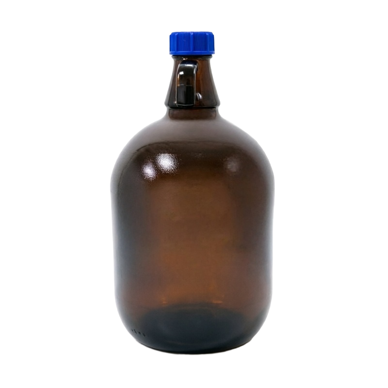
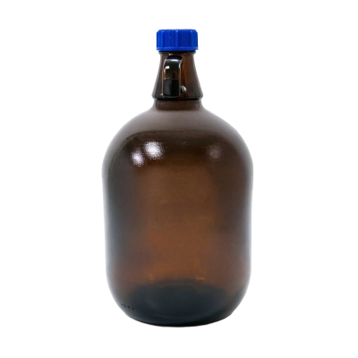
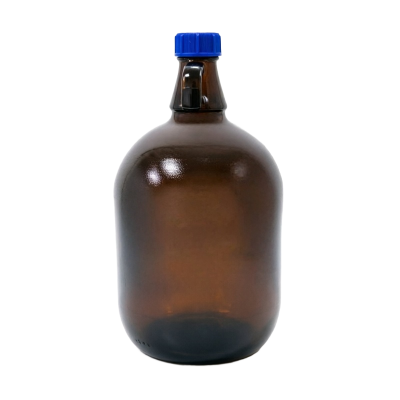
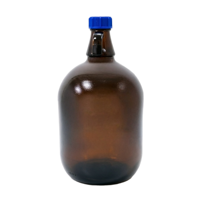
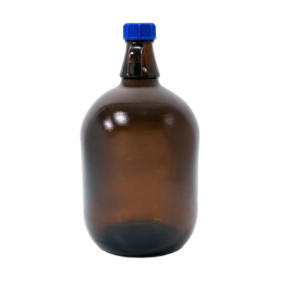
Our negative photoresist series is based on the proven cycloalkene rubber / diazo photosensitive system, designed for G-line (436nm) and I-line (365nm) exposure wavelengths. With high adhesion to silicon, metal, and oxide substrates, excellent etch resistance, and reliable pattern transfer, it is the ideal choice for discrete device manufacturing including mesa and planar processes. Our YY-N210 and YY-N220 series products offer tailored solutions for diverse process requirements, from high-adhesion mesa structures to high-resolution planar patterning.
• High Adhesion – Excellent adhesion to silicon, oxide, and metal substrates.
• Excellent Etch Resistance – High selectivity against common etchants including CF4, O2, and Ar-based plasmas.
• High Resolution – Resolution down to 1.0 μm with steep sidewall profiles.
• Wide Process Window – Generous exposure latitude and bake tolerance for stable production.
• Good Step Coverage – Superior conformal coverage on non-uniform surfaces and stepped topographies.
Parameter | Specification |
Exposure Wavelength | 365nm (I-line) / 436nm (G-line) |
Resolution | 1.0 – 3.0 μm |
Film Thickness | 1.0 – 5.0 μm (adjustable by viscosity and spin speed) |
Sensitivity | 50 – 200 mJ/cm² (depending on grade) |
Developer | NMP (N-Methyl-2-pyrrolidone) or 2.38% TMAH (aq.) |
Soft Bake | 90 – 110°C / 60 – 120s |
Hard Bake | 120 – 150°C / 60 – 120s |
Metal Ion Content | ≤10 ppm |
Viscosity | 20 – 80 cP (adjustable by formulation) |
Shelf Life | 12 months (stored at 0–10°C, dark) |
• Discrete Device Mesa Process – Power diodes, rectifiers, and Zener diodes requiring high step coverage and strong etch resistance.
• Discrete Device Planar Process – Transistors (BJT, MOSFET), thyristors (SCR), and photodiodes requiring high resolution and fine patterning.
• Passivation Layer Patterning – Window opening in SiO2 and Si3N4 passivation layers for metallization and bonding pads.
• Isolation Region Definition – Field isolation and device isolation patterning in power semiconductor devices.
• MEMS & Sensors – Thick-film and high-aspect-ratio structure fabrication for micro-electromechanical systems and sensors.
Grade | Resolution | Film Thickness | Best For |
Standard Grade (YY-N210) | 2.0 μm | 2.0 – 5.0 μm | Mesa process, high adhesion, general discrete devices |
High-Resolution Grade (YY-N220) | 1.0 μm | 1.0 – 3.0 μm | Planar process, fine patterning, high-resolution devices |
High-Etch-Resistance Grade (YY-N230) | 2.0 μm | 2.0 – 5.0 μm | Aggressive etch processes, high selectivity requirements |
Improved Coverage Grade (YY-N260) | 2.0 μm | 2.0 – 5.0 μm | Stepped surfaces, non-uniform topography, mesa structures |
• Stable Supply Chain – Consistent batch-to-batch quality with reliable production capacity.
• Export-Ready – Complete COA, SDS, and export compliance documentation provided.
• Technical Support – Process optimization guidance and on-site application support.
• Samples Available – Free evaluation samples for R&D validation and process qualification.

Contact: Jiang.S
Phone: +86-19304758719
E-mail: info@yycheme.com
Whatsapp:+86-18966258719
Add: Liushi Town, Yueqing City, Wenzhou City, Zhejiang Province, 325604, China