Email: info@yycheme.com Tel: +86-19304758719


Email: info@yycheme.com Tel: +86-19304758719
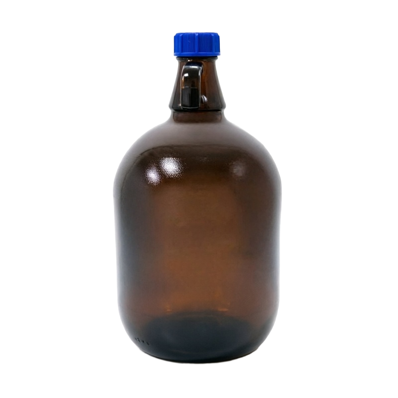
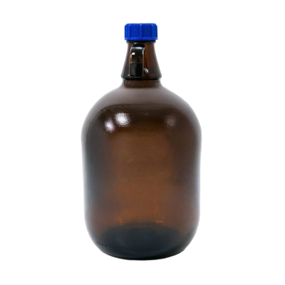
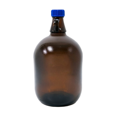
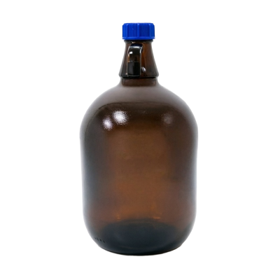
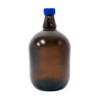
Our Thick-Film Photoresist series is a positive-working photoresist based on the proven Novolac resin / DNQ (Diazonaphthoquinone) photosensitive system, engineered for film thickness ranging from 5μm to 20μm. Designed specifically for advanced packaging, LED deep trench, and MEMS fabrication, this product delivers exceptional step coverage over complex topographies, high aspect ratio profiles, and superior etch resistance. With ultra-low metal ion contamination (≤10ppb) and excellent adhesion to silicon, glass, oxide, and metal substrates, it is the ideal choice for demanding thick-film lithography applications in semiconductor manufacturing.
· Thick Film Capability: Achieves uniform film thickness from 5μm to 20μm with excellent coating uniformity across large-area substrates, suitable for spin-coating and spray-coating processes.
· Excellent Step Coverage: Superior conformality over stepped topographies and deep trench structures, significantly reducing development defects and pinhole formation.
· High Aspect Ratio: Enables vertical sidewall profiles with aspect ratios up to 10:1, ideal for deep trench etching in LED and MEMS applications.
· Ultra-High Purity: Metal ion content controlled at ≤10ppb, preventing contamination during wafer fabrication and ensuring device reliability.
· Superior Etch Resistance: Excellent resistance to both wet and dry etching processes, serving as a robust masking layer with high selectivity against silicon, silicon dioxide, and metal layers.
· Wide Process Window: Generous depth of focus (DOF) and exposure latitude for high yield and process stability in production environments.
Parameter | Specification |
Type | Positive Photoresist |
Film Thickness | 5 – 20 μm |
Exposure Wavelength | 365nm (I-line) / 405nm (G-line) |
Resolution | 3.0 – 5.0 μm |
Metal Ion Content | ≤10 ppb |
Developer | 2.38% TMAH (aq.) or IVF |
Solvent | PGMEA |
Soft Bake | 90 – 110°C, 1 – 3 min |
Post-Exposure Bake (PEB) | 100 – 120°C, 1 – 3 min |
Hard Bake | 120 – 150°C, 2 – 5 min |
Shelf Life | 12 months (stored at 0–10°C, dark) |
· Advanced Packaging: RDL (Redistribution Layer), Bumping, TSV (Through-Silicon Via), Fan-Out Wafer-Level Packaging (FOWLP), and 2.5D/3D heterogeneous integration
· LED Manufacturing: Deep trench etching for LED chips, current blocking layers, optical isolation structures, and surface texturing
· MEMS & Sensors: Micro-electro-mechanical system patterning, deep silicon etching, pressure sensors, accelerometers, gyroscopes, and bio-sensors
· Power Semiconductors: MOSFET, IGBT, SiC, GaN device fabrication including isolation structures and passivation layer patterning
· General Purpose: Thick-film masking, electroplating molds (LIGA process), surface passivation, and micro-structure fabrication
Grade | Film Thickness | Resolution | Best For |
Standard Grade (YY-3520) | 5 – 10 μm | 5.0 μm | General advanced packaging, LED trench etching |
High-Thickness Grade (YY-3520H) | 10 – 20 μm | 3.0 μm | Deep trench MEMS, high aspect ratio structures |
High-Resolution Grade (YY-3520R) | 5 – 8 μm | 3.0 μm | Fine pitch RDL, advanced packaging, fine patterning |
Anti-Reflective Grade (YY-3520AR) | 5 – 15 μm | 3.0 – 5.0 μm | High-reflectivity substrates, multi-layer stacks |
· Stable Supply Chain: Consistent batch-to-batch quality with reliable production capacity to support large-scale manufacturing
· Export-Ready: Full COA, SDS, and export compliance documentation provided for global shipments
· Technical Support: Process optimization guidance and on-site application support available from our experienced engineering team
· Samples Available: Free evaluation samples for R&D verification and process qualification

Contact: Jiang.S
Phone: +86-19304758719
E-mail: info@yycheme.com
Whatsapp:+86-18966258719
Add: Liushi Town, Yueqing City, Wenzhou City, Zhejiang Province, 325604, China